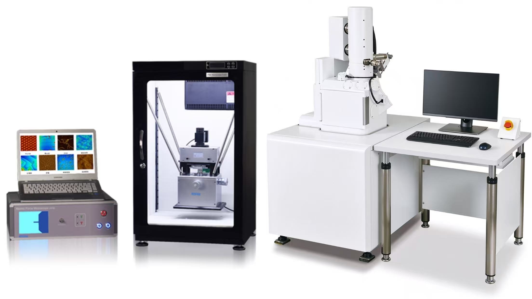
Choosing the most suitable tool for high-resolution analysis of surfaces is the key issue for many research laboratories and industry inspection facilities in contemporary times. Engineers and material specialists often encounter various problems when choosing between AFM and SEM due to dimensional issues, sample preparation needs, and budget constraints:
- Dimensional Ambiguity: Whether the 2D grey-scale shades provide quantitative 3D data on feature heights.
- Sample Modification: Experiencing damage to their samples or artifacts due to the rigorous requirement of conductive coatings.
- Operational Delays: Waste considerable time seeking nanometer-wide target areas in the samples.
- Budget Mismatching: Deal with high costs of equipment acquisition and laboratory expenses.
To cope with these analytical difficulties, OPTOEDU—an innovative international microscope producer with more than 25 years of optical science experience—provides you with top-notch imaging instrumentation and all its accessories at reasonable prices, technical support, and a worldwide 3-year warranty period for analyzing AFM vs. SEM.
3D Topographic Analysis vs. Electron Beam Imaging
Force probe interactions versus focused electron beams can be distinguished by a full understanding of dimensional outputs and signaling processes. For a comparison between the two technologies, it is first essential to figure out which one needs more attention – height or electron contrast.
Principles of AFM 3D Surface Topography and SEM 2D Projections
Each of the imaging methods employs different physical principles in interacting with the properties of the samples.
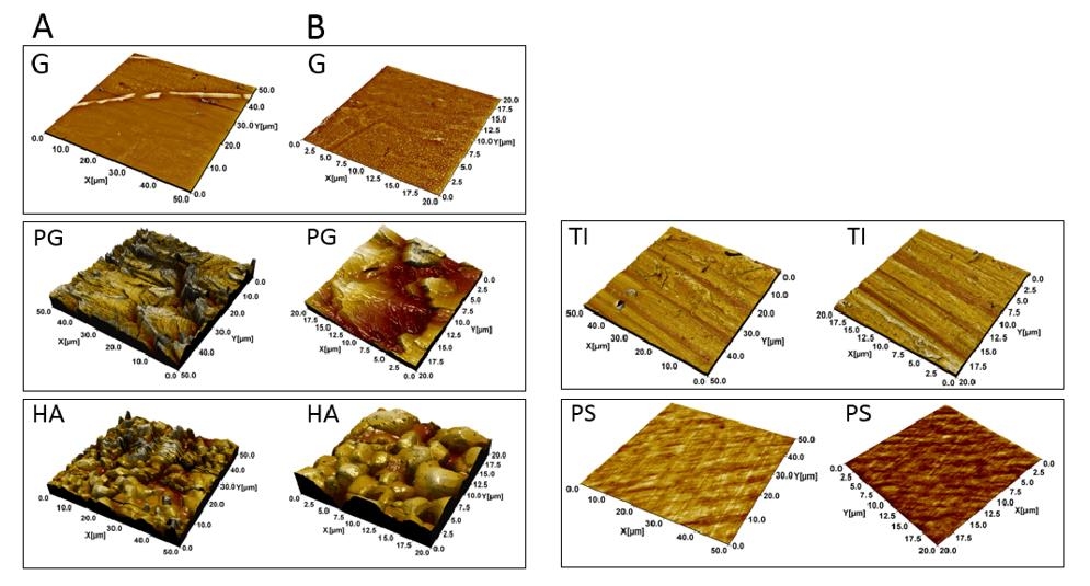
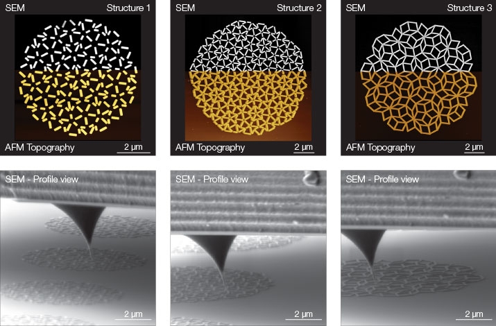
- Dimensionality: AFM 3D surface topology gives true quantitative Z-height coordinates based on physically scanning the micro-cantilever probe tip over the sample surface, while SEM gives 2D intensity projections based on electron scattering.
- Surface Roughness: AFM surface roughness measurement gives precise sub-nanometer Ra, Rq, and peak-to-valley measurements, making AFM vs SEM for surface roughness measurements better suited for quantitative metrology applications.
- Resolution Scale: AFM vs SEM resolution comparison shows that although SEM resolution is extremely good in lateral scale (1-5 nm), AFM can give sub-nanometer vertical resolution (<0.1 nm).
Practical Application Scenarios in Surface Characterization
Quality assessment and material design in industries require an appropriate technique for nanoscale surface characterization.
- Semiconductor Wafer: Assessing trench depth and polishing quality in silicon wafers needs proper atomic force microscopy against SEM for assessing micro-roughness and height of features.
- Polymer Thin Film: Characterizing nanoscale surfaces on soft polymer films indicates localized elasticity variations without inducing surface charging.
Sample Preparation Requirements and Operational Constraints
The efficiency of workflow and preservation of samples depend on the requirements for sample preparation prior to imaging in each case. Sample preparation for AFM vs SEM is particularly critical when samples are fragile, insulating, or chemically sensitive.
AFM vs SEM Sample Preparation Demands
Pre-imaging treatments will determine if delicate samples will have their natural morphology preserved.
- Coating Considerations: SEM specimen preparations need gold or carbon sputtering as a treatment to avoid electron beam charge buildup when non-conductive specimens are imaged.
- Atmosphere: AFM specimen preparations need only a minimum setup because non-destructive imaging is performed in ambient atmosphere or liquids.
- Preservation Consequences: Comparison of AFM and SEM specimen preparations reveals that AFM retains the native surface characteristics for further tests.
Application Scenarios Across Sensitive Materials
Evaluating non-conductive and fragile structures requires tailored operational environments.
- Biological Macromolecules: Comparing AFM vs SEM for delicate DNA or protein structures demonstrates that ambient AFM imaging prevents dehydration artifacts.
- Insulating Ceramics: Examining ceramic fractures without conductive sputtering eliminates fake surface textures introduced by metal coatings and reduces the preparation burden associated with SEM sample coating requirements.
Cost of Ownership and Long-Term Value Analysis
Apart from the initial cost of buying the equipment, the operating costs and infrastructure requirements are factors that determine the total cost of ownership. The cost comparison between AFM and SEM should include the following considerations.
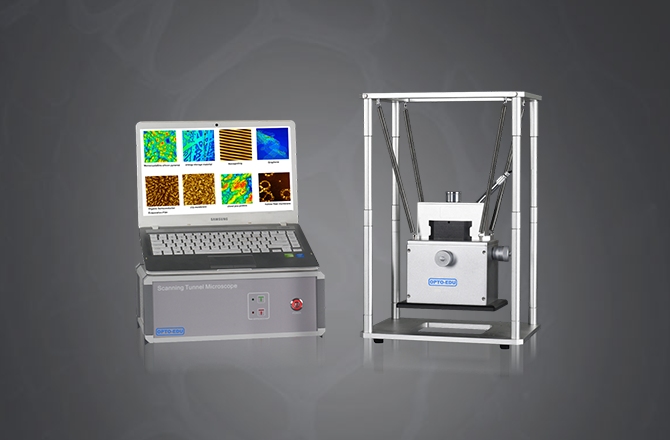
Atomic Force Microscope Cost vs. SEM Infrastructure Investments
A comprehensive cost analysis will have to factor in facility preparation, vacuum maintenance, and consumables.
- Initial Capital Cost: The capital cost of atomic force microscopes is usually low because there is no need for costly high-vacuum turbomolecular pumps in AFM.
- Operational Overhead Cost: A detailed comparison between AFM and SEM costs will show reduced operational costs of the facility due to electrical requirements and lower facility needs.
OPTOEDU Products, Technology, and Customized Service Support
OPTOEDU provides reliable hardware with expert global services as well as custom-designed setups.
- Advanced Hardware: The A62 series atomic force microscopefrom OPTOEDU has high-precision piezo-scanners as well as a spring-suspension shockproof system that ensures sub-nanometer stability.
- Customized Engineering: In addition, OPTOEDU provides customized hardware modules, customized probe holders, and customized analysis software packages based on research requirements.
- Warranty & Service: All OPTOEDU systems come with a factory-backed guarantee as well as a 3-year warranty period.
Integrated Solutions: When to Pair AFM with Optical Microscopy
Optical guiding and force sensing at the nanometer scale close the distance between macroscopic positioning and atomic-scale measurement. The optical atomic force microscope can decrease target positioning time without compromising its quantitative surface measurement capabilities.
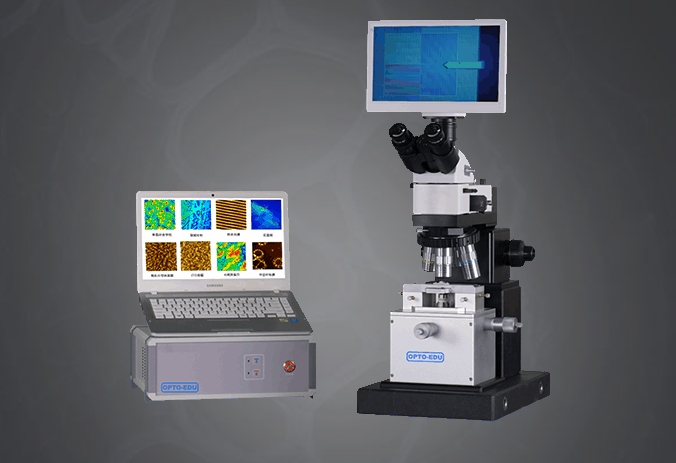
Synergizing Optical AFM Microscope Systems for Rapid Workflow
The combination of physical probe scanning and optical vision greatly increases productivity.
- Macro-to-Micro Navigation: With the use of integrated AFM optical microscopy, operators can quickly identify targets using bright-field or fluorescence optics prior to using the AFM probe.
- System Integration: The optical atomic force microscope system integrates optical 2D navigation with 3D physical surface profiling.
- Integrated Workflow: Using an optical atomic force microscope system greatly reduces inspection cycle time, as there is no need for blind probe placement.
Industry Applications and Customized Workflows
Dual-mode systems facilitate comprehensive failure analysis in both industrial and academic laboratories.
- Microelectronics Quality Control: Optical identification of microcircuit defects, along with immediate determination of pit depth by AFM 3D topography, makes the defect analysis process efficient.
- Customizable R&D Platforms: OPTOEDU offers customizable optical atomic force microscope systems with customized sample stages and software measurement algorithms.
Contact OPTOEDU for Specialized Microscopy Solutions
Seeking improved imaging techniques at the nanometer level by means of highly accurate, yet affordable, equipment? Feel free to get in touch with our engineers from OPTOEDU for professional advice on choosing models, to have a demonstration session, or to design your own instruments according to special research needs.
FAQ
Q: What is the main benefit of AFM over SEM regarding roughness measurements?
A: The main difference between AFM and SEM for roughness measurement lies in the nature of the data. AFM gives qualitative 3D height map information with sub-nanometer accuracy in vertical dimensions, while SEM gives 2D contrast information only, without any metrology. In case of precise AFM surface roughness measurement, the obtained height map allows calculating Ra, Rq, and peak-to-valley parameters.
Q: Should all samples that are not conducting need additional coating for SEM and AFM?
A: SEM needs to use an additional sputtering procedure for most non-conducting samples to prevent charging effects, but AFM allows scanning of non-conducting samples as well without any special procedures.
Q: How is an integrated optical atomic force microscope able to increase the speed of the test process?
A: The integrated optical AFM microscopy utilizes the optical imaging technique to find the exact point of interest so that the physical probe can be positioned accurately without the need to search blindly.
Q: Is OPTOEDU able to offer a customized microscope system solution for industrial purposes?
A: Yes. OPTOEDU offers customized hardware stages, customized optical modules, customized software routines, and optical atomic force microscope systems according to laboratory requirements.