AFM vs SEM is not a question of which microscope is universally better; it is a question of what kind of surface evidence a lab needs. SEM delivers detailed visual images of surface appearance, while AFM measures probe-sample interaction to create quantitative three-dimensional topography. When roughness, step height, local texture, or nanoscale surface morphology matters, an atomic force microscope can add data that SEM images alone do not provide.
For many materials labs, the strongest workflow is comparative rather than competitive. SEM can reveal particles, fractures, coating defects, and microstructures quickly, while AFM can measure the height profile of a selected region. OPTOEDU A62 AFM systems fit this workflow by giving users contact, tapping, optical navigation, and research-level scan options for surface analysis after a target area has been identified.
AFM vs SEM: What Each Microscope Actually Measures
SEM Shows Surface Appearance and Morphology
The scanning electron microscope creates an image through the use of electrons and hence it is very useful in creating an image at higher magnifications. The scanning electron microscope is used to investigate samples such as particles, cracks, fibers, fractures, coatings, and microstructures where the image answers the primary question. It has good depth of field impressions.The limitation is that SEM contrast is not the same as direct height measurement. Charging behavior, coating, conductivity, vacuum conditions, detector choice, and sample preparation can all influence the image. SEM can support surface analysis, but it should not be treated as a direct substitute for AFM topography when the decision depends on roughness, height, or a three-dimensional surface profile.
AFM Measures Height, Force, and Surface Texture
An atomic force microscope scans a sharp tip across or near the sample and tracks cantilever movement caused by tip-sample forces. The result is a height map that can show surface roughness, steps, particles, grains, and fine texture in three dimensions. This makes AFM especially useful when a lab needs quantitative surface data rather than a visual image alone.
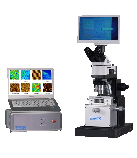
The OPTOEDU A62.4505 optical atomic force microscope strengthens this workflow by combining optical and AFM imaging in one system. It supports optical 2D measurement and AFM 3D measurement at the same time, with a 10x eyepiece, LWD APO 5x, 10x, 20x, and 50x objectives, a 5.0M camera, a 10-inch LCD monitor, LED Kohler illumination, and coaxial coarse and fine focusing.
Sample Preparation Differences Between AFM and SEM
SEM Preparation Can Change the Workflow
SEM commonly requires attention to vacuum compatibility, conductivity, charging, and surface coating. These requirements are manageable in many industrial and research settings, but they can add preparation steps before imaging. For conductive materials, hard coatings, and stable dry samples, SEM remains a fast way to document surface features and compare visible defects.
The preparation burden becomes more important when a sample is soft, hydrated, poorly conductive, or easily altered. Coating or vacuum exposure may not be appropriate for every specimen. In those cases, AFM can be attractive because it measures with a probe and can often work with less image-driven preparation, depending on the sample and chosen scan mode.
AFM Preparation Focuses on Stability and Scan Area
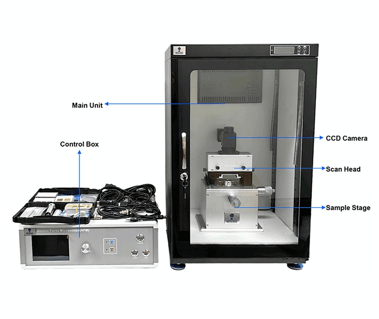
AFM preparation is usually about mechanical stability, surface cleanliness, and choosing a scan area that matches the feature size. The OPTOEDU A62.4503 research-level atomic force microscope lists a 50 x 50 um XY scan range and 5 um Z range, giving research users more room to explore broader surface features before moving into fine measurement. Its 25 x 25 mm stage moving range also supports practical sample navigation.
Resolution, Data Type, and Interpretation
Why SEM Resolution Is Visually Powerful
SEM is visually powerful because it can show fine surface details over a useful field of view. For many users, the image is immediately readable: a particle, pore, crack, fiber, or coating flaw can be seen and documented. This is one reason SEM remains a core tool for failure analysis, quality control, and materials research.
However, SEM image detail should be interpreted as visual and contrast information. It may suggest texture or height, but it does not automatically provide a calibrated 3D topographic map. When the question is whether one coating is rougher than another, or how high a step edge is, AFM gives a more direct measurement route.
Why AFM Data Is Quantitative
AFM data is quantitative because the scan records surface height as the probe follows the sample. This allows users to analyze roughness, line profiles, step height, particle dimensions, and surface morphology. It is especially useful for thin films, polished materials, semiconductor-related samples, coatings, and microstructures where height variation is central to the result.
Optical navigation still matters because AFM scan areas are relatively small compared with the whole specimen. OPTOEDU A62.4505 helps bridge that gap by letting the user identify a visible feature optically, then measure the selected area with AFM 3D data. In practice, this makes AFM and optical positioning work together while SEM remains useful for broader visual documentation.
Choosing an OPTOEDU AFM for an AFM vs SEM Workflow
Choose A62.4505 When Visual Navigation Matters
A62.4505 is the best fit when the workflow needs optical location and AFM measurement in one platform. It is useful when the operator must first find a visible target, then measure surface height, roughness, or morphology in the same region. This is a practical complement to SEM workflows that identify defects visually before a lab needs direct topographic data.
Choose A62.4501 for Routine Surface Measurement
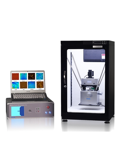
The OPTOEDU A62.4501 basic-level atomic force microscope suits users who need contact and tapping modes within a compact scan range. Its listed XY scan range is 20 x 20 um, with a Z range of 2.5 um, XY resolution of 0.2 nm, and Z resolution of 0.05 nm. It is a practical choice for routine roughness, coatings, prepared samples, and training-oriented surface measurement.
Choose A62.4503 for Research-Level Mapping
A62.4503 is stronger when the lab expects larger scan areas, taller features, or more research-oriented exploration. Its listed 50 x 50 um XY scan range and 5 um Z range give users more measurement space than a compact routine system. When SEM has already identified a feature of interest, A62.4503 can help quantify the height and texture of that region.
Where AFM and SEM Work Best Together
Thin Films, Coatings, and Roughness
Thin films and coatings are natural candidates for AFM and SEM comparison. SEM can show visible defects, particles, cracks, and coating coverage, while AFM can quantify roughness and local height variation. Used together, the two methods connect what the surface looks like with how the surface is actually shaped.
Failure Analysis and Quality Control
In failure analysis, SEM can quickly document the visible condition of a damaged or contaminated area. AFM can then measure whether that area has a raised particle, a depression, a scratch profile, or a roughness change. This combination is useful when a report needs both visual evidence and numerical surface information.
Education and Method Selection
For education, AFM vs SEM is a useful way to teach instrument selection. Students can see that SEM is strong for visual morphology, while AFM is strong for 3D surface measurement and tip-based interaction. OPTOEDU A62 systems support this learning path by linking optical navigation, contact mode, tapping mode, and nanoscale surface analysis.
Conclusion
AFM vs SEM should be decided by the data the laboratory needs. SEM is the stronger choice for high-magnification visual surface documentation, broad morphology review, and fast inspection of visible features. AFM is the stronger choice when the task requires quantitative three-dimensional topography, roughness, step height, or local surface texture. OPTOEDU A62 AFM systems give users practical AFM options that can complement SEM rather than compete with it.
Explore the OPTOEDU A62 AFM configuration that adds direct 3D surface measurement to your SEM-based analysis workflow.
FAQ
Q: What is the main difference between AFM and SEM?
A: SEM generates high-resolution images of surface characteristics by the use of electrons, whereas AFM utilizes a probe in order to determine the surface topography and tip-sample interactions. SEM is excellent for morphology and documentation. AFM is stronger when the lab needs quantitative 3D topography, roughness, step height, or local surface texture.
Q: Is AFM better than SEM for surface roughness?
A: AFM is usually more direct for surface roughness because it measures height changes across the scanned area. SEM can show surface texture visually, but the image does not automatically provide a calibrated topographic profile. Many labs use SEM to locate a region and AFM to quantify it.
Q: Can AFM replace SEM in materials analysis?
A: AFM should not be considered an entire substitute for SEM. The SEM is best used for broad viewing and surface imaging at higher magnifications, whereas the AFM is ideal for the direct measurement of height on selective regions. The two methodologies complement each other, especially in coating, thin film, particle, and microstructure applications.
Q: Which OPTOEDU AFM fits an AFM and SEM comparison workflow?
A: OPTOEDU A62.4505 fits workflows that need optical navigation plus AFM 3D measurement. A62.4501 supports compact routine contact and tapping measurement, while A62.4503 offers a larger 50 x 50 um XY scan range and 5 um Z range for research-level surface mapping after SEM inspection.