A 3D measuring microscope helps PCB and semiconductor teams inspect height, surface texture, edge geometry, and wider sample areas without relying only on flat images. It becomes most valuable when a part has uneven solder, polished metal, micro grooves, bonded pads, or features that need both magnified detail and spatial measurement.
For industrial laboratories, the practical question is not whether magnification is high enough. The stronger question is whether the microscope can keep focus, lighting, movement, and measurement consistent across repeated samples. OPTOEDU‘s M20 motorized industrial systems answer that need with motorized positioning, 2D and 3D imaging, image stitching, and controlled illumination for difficult surfaces.

Why a 3D Measuring Microscope Matters in Electronics Inspection
PCB and semiconductor inspection often sits between optical observation and dimensional analysis. A flat image can show a defect, but it may not explain whether the feature rises above the surrounding surface, sinks below it, or changes shape across the board. That is why a 3D measuring microscope is useful for solder bumps, wire bonding areas, polished component surfaces, etched structures, and other small features where depth changes matter.
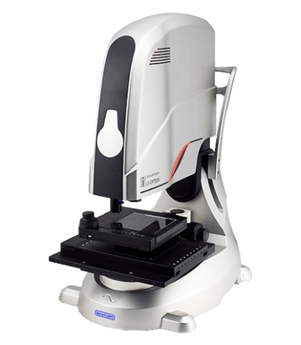
The OPTOEDU M20.0910 is positioned as a 3D measurement microscope with a telecentric continuous zoom system, six illumination modes, a rotating stage, angle sensing, and 2D/3D software. Its role is clear: keep magnification, lighting, and measurement aligned when the operator needs to move from overview inspection to detail confirmation.
Where PCB and Semiconductor Samples Challenge Ordinary Microscopy
Height differences across solder, pins, and pads
Uneven electronic samples are difficult because the point of interest may not sit on one focal plane. Solder joints, connector pins, package edges, coatings, and trace damage can all create height differences across a small field. If the operator keeps refocusing manually, the final record may show different points clearly but never present the whole surface in a way that supports comparison.
A 3D measuring microscope with Z-series capture and reconstruction helps connect focus information with surface shape. It gives the user a clearer way to judge whether a defect is only visual, whether a raised point may affect contact, or whether a recessed feature deserves further analysis.
Wider fields that still need high magnification
A single high-magnification field rarely covers an entire inspection region. This is common on circuit boards and semiconductor samples, where a user may need to inspect a larger pad group, a repeated pattern, or a longer surface mark. Image stitching matters because it keeps the local detail connected to the surrounding structure.
M20.0910 supports image stitching, multi-area shooting, auto measurement, and 2D/3D imaging software. In practice, that means the operator can build a broader visual record without abandoning microscopic detail. The same logic applies to OPTOEDU M20.5830, which supports full automatic 2D large image stitching and 2D plus 3D multilayer image stitching.
How Motorized Scanning Improves Repeatability
XY movement for large-area inspection
Repeatability begins with movement. When a sample is moved by hand, small differences in position, focus, and angle can change the final image. A motorized stage helps turn inspection into a repeatable route rather than a set of isolated snapshots.
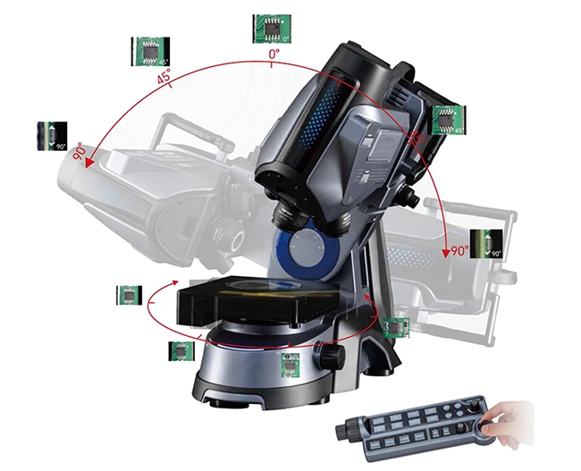
The M20.5830 combines a motorized XY stage with a 100 mm by 100 mm moving range and 0.05 um resolution. That level of motion control is useful when the same sample type must be checked across many regions, or when a large field needs to be stitched from smaller images.
Z-axis control for height and profile data
Height measurement depends on controlled vertical movement. The M20.5830 includes a motorized Z-axis with a 100 mm movement range and 0.1 um resolution. For uneven samples, this supports layered image capture, extended depth of field, 3D reconstruction, and measurement of spatial features.
This matters for industrial samples because surface problems are rarely shaped like simple lines. A scratch may have depth, a chip may have a raised edge, and a solder area may show both spread and height. Z-axis control makes those observations more structured.
Lighting Controls Surface Detail
Lighting is often the difference between seeing a surface and understanding it. Reflective metal, dark circuit materials, transparent coatings, and fine scratches respond differently to coaxial, ring, oblique, polarized, or transmitted light. The M20.0910 product page identifies coaxial epi, coaxial oblique, annular, segmented annular, mixed, and transmitted illumination.
The M20.5830 expands this idea with bright field, dark field, inclined four-zone light, polarized light, optional DIC, and optional transmitted light. For PCB and semiconductor inspection, this lets the user reveal edges, reduce glare, and compare surface behavior under different lighting conditions without changing the entire inspection setup.
What OPTOEDU Adds to Industrial Inspection Workflows
OPTOEDU’s industrial M20 line is useful because it connects optics, movement, lighting, imaging, and software around actual inspection decisions. The M20.5830 reaches a 12x to 8000x system magnification range and uses a 16:1 motorized zoom body, a built-in 12.0M USB 3.0 digital camera, and APO long-working-distance objectives. The system is built for 3D optical imaging, stitching, measurement, tilt viewing, and software-controlled focus.
The M20.0910 is a more direct fit when the search intent centers on a 3D measuring microscope for industrial inspection. Its telecentric zoom, 20x to 7500x motorized magnification switch, multi-illumination configuration, rotating stage, angle sensing, and 2D/3D software all support the same practical goal: clearer inspection records with less dependence on manual adjustment.
Selection Advice for Real Inspection Tasks
A 3D measuring microscope should be chosen around the sample, not around the longest parameter list. If the sample is wide and repeated, prioritize motorized XY travel, stitching, and route consistency. If the sample is tall or uneven, prioritize Z-axis control, depth reconstruction, and extended depth of field.
If the inspection surface is reflective, lighting flexibility becomes more important than magnification alone. For electronics and semiconductor work, a system that lets the user compare coaxial, oblique, ring, polarized, or transmitted light can reveal detail that one illumination method would hide.
Conclusion
A 3D measuring microscope gives electronics and semiconductor teams a more useful view of small parts because it connects magnified detail with height, position, lighting, and repeatable measurement. OPTOEDU’s M20.0910 and M20.5830 support this work through telecentric zoom, motorized control, 2D/3D imaging, image stitching, and flexible illumination.
Explore the OPTOEDU industrial microscope options to match the inspection method to the sample geometry, surface material, and measurement workflow.
FAQ
Q: What is a 3D measuring microscope used for in PCB inspection?
A: It is used to inspect surface height, solder shape, component edges, scratches, coatings, and broader board areas that need both magnified detail and spatial information. It helps operators move beyond a flat image and judge whether a feature has depth, raised edges, or measurable surface variation.
Q: Why does image stitching matter for semiconductor inspection?
A: Semiconductor and PCB features often extend beyond one high-magnification field. Image stitching combines smaller fields into a wider view while preserving detail. This helps users inspect repeated patterns, longer marks, bonding areas, or pad groups without losing the relationship between local defects and the larger structure.
Q: Is magnification the most important specification?
A: Magnification is important, but it is not enough by itself. Lighting, working distance, motorized movement, Z-axis control, camera quality, and measurement software strongly affect inspection quality. A useful system should match the sample’s surface, height range, reflectivity, and repeatability needs.
Q: When should a lab consider OPTOEDU M20.5830 instead of M20.0910?
A: M20.5830 is better suited when the workflow needs motorized XYZ movement, a tilt stand, 12x to 8000x system magnification, large-area stitching, layered 3D imaging, and multiple illumination modes. M20.0910 is a strong fit when the main need is telecentric 3D measurement with controlled lighting and software-supported inspection.